the Creative Commons Attribution 4.0 License.
the Creative Commons Attribution 4.0 License.
 | 11 Feb 2021
Research on a UV-assisted chemical modification strategy for monocrystalline silicon
Yinghui Ren
Kexin Li
Wei Li
Xu Han
Xiaoman Liu
A novel UV-assisted chemical modification (UVA-CM) strategy is proposed for micro-grinding monocrystalline silicon based on UV photocatalysis theory in order to develop a combined machining technology. Comparative experiments are carried out between a single heating chemical modification (H-CM) strategy and a hybrid UVA-CM strategy. The effects of different modification strategies on modification degree and mechanical properties of a modified layer are evaluated by inductively coupled plasma mass spectrometry (ICP), Raman spectral analysis, nanoindentation test, and scratch test. The experimental results show that silicate substance is generated on the modified layer surface via the UVA-CM technique. The modified layer under UVA-CM is thicker than that under the H-CM strategy, which also presents relatively lower nanohardness. With the same scratch condition, the modified layer under UVA-CM contributes to inhibiting lateral crack propagation. It is demonstrated that the liquid–solid chemical modification effect is obviously enhanced through UV advanced oxidation reaction. The UVA-CM strategy will contribute to developing a novel hybrid chemo-mechanical process for micro-grinding monocrystalline silicon.
- Article
(6817 KB) - Full-text XML
- BibTeX
- EndNote


Monocrystalline silicon is a typical hard–brittle semiconductor material. Due to its excellent mechanical properties, monocrystalline silicon has been widely used in various fields such as microfluidics, biomedical systems, and optical fields (Aurich et al., 2019). Micro-grinding is one of the emerging ultra-precision machining technologies for the fabrication of micro-size parts of hard–brittle semiconductor materials. However, due to the inherent hard and brittle property of silicon materials, the machining defects such as micro-pits, broken edges are easily generated (Aurich et al., 2015). To reduce mechanical damage and improve machining quality, chemo-mechanical synergism techniques such as chemical mechanical grinding (CMG) and chemical mechanical polishing (CMP) were developed for ultra-precision machining of hard–brittle materials by weakening the hard and brittle property of materials (Zhou et al., 2009; Yuan et al., 2010). The chemical mechanical hybrid process weakens hard–brittle material mainly through two kinds of reaction methods, namely liquid–solid reaction (e.g., CMP) and solid–solid reaction (e.g., CMG). They are mostly applied in the planarization technology of the wafer in IC manufacturing. Several researchers also proposed the introduction of chemical mechanical hybrid processing of liquid–solid reaction into the complex structural part processing. Qiu et al. (2010, 2013) and Lu (2013) developed a special grinding fluid with a chemical effect for chemical mechanical grinding of glass through liquid–solid reaction, but the chemical modification time was up to 5–8 h. From the research results, it is found that the existing technology is not efficient enough and that the suitable type of processed materials is limited. There are also some unsolved bottleneck problems limiting the development of chemical mechanical hybrid processing, such as how to speed up chemical modification reaction, how to determine the threshold condition of different material chemical modifications, and how to increase the thickness of the chemical modified layer.
Some researchers focused on the UV advanced oxidation reaction of hydrogen peroxide (H2O2) to increase hydroxyl radical content based on photocatalysis theory in a chemical mechanical hybrid processing technique. Ishimarua et al. (2012) designed a UV-assisted polishing method to realize chemo-mechanical material removal. Kubota et al. (2012a) discussed the process of polishing SiC surfaces under UV irradiation in H2O2 solution to improve mechanical machining quality. Ye et al. (2017) added UV-LED light during the 4H-SiC wafer chemical mechanical polishing and then obtained 0.0586 nm surface roughness. Therefore, by introducing UV advanced oxidation reaction to improve the chemo-mechanical hybrid process, the mechanism, method, and strategy of the UV-assisted technology are worthy of study.
Generally, in order to study material removal behaviors, researchers conducted a single-point scratch test to simulate the grinding process and evaluate the material removal mechanism. Li et al. (2017) used the nanoindentation system to perform a single-particle scratch test with different cutting depths and calculated the critical depth of the elastic–plastic transition of SiC ceramics. Alamgir et al. (2019) analyzed mechanical and tribological properties of alumina films with a thickness of 100 nm, which is prepared by atomic layer deposition on Si (100) substrates, using nanoindentation and scratch tests. It is an effective method to evaluate the effect of chemical modification strategy on material removal behaviors of the modified layer through a scratch test to simulate a micro-grinding process.
In this paper, a novel UV-assisted chemical modification (UVA-CM) strategy was proposed based on UV photocatalysis theory. A set of comparative experiments was conducted to evaluate the chemical modification effect on liquid–solid chemical reaction of monocrystalline silicon, which was dipped into a special alkaline chemical modification solution under different strategies. The mechanical properties and material removal behavior of the modified layer were also analyzed through chemical analysis, a nanoindentation test, and a single-point scratch test.
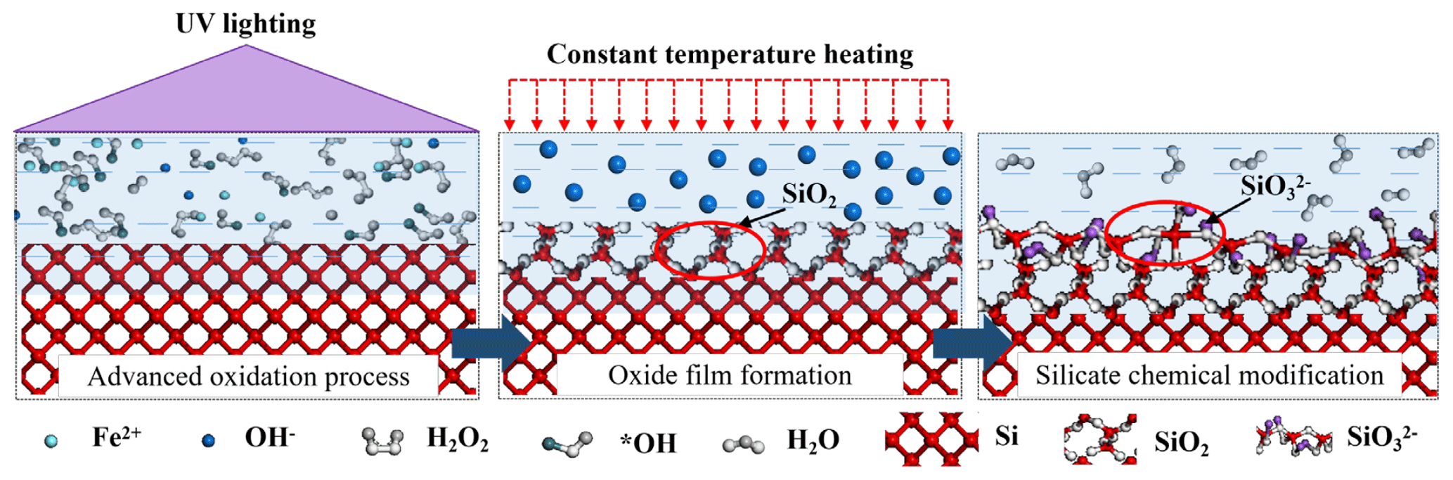
From published monocrystalline silicon CMP reports, chemical reaction mainly occurred between monocrystalline silicon and strong oxidizing hydroxyl radicals (•OH) catalyzed by a Fenton reagent as shown in Eqs. (1)–(4) (Kubota et al., 2012b; Lu et al., 2017). However, the Fe2+ in the Fenton reagent needs to be continuously supplemented, otherwise the hydroxyl radicals cannot keep resolving. Applying UV light to irradiate the H2O2 aqueous solution, the UV advanced oxidation reaction occurs and generates •OH-based photocatalytic theory (Zhang et al., 2003; Zhou et al., 2014). The UV advanced oxidation reaction promotes the •OH reaction cyclic according to Eqs. (5)–(7). Additionally, the UV photocatalysis in an alkaline environment can transfer Fe(OH)2 to Fe2+ according to (Eq. 8), whose oxidizability can further enhance without additional supplying a Fenton reagent.
Thus, a UV-assisted chemical modification (UVA-CM) strategy is proposed to promote the reaction efficiency between chemical modification solution and monocrystalline silicon in this paper. The UVA-CM process is implemented in two stages as shown in Fig. 1. In the first stage, the monocrystalline silicon wafer is immersed in a special alkaline chemical solution containing a Fenton reagent. After that, the UV light directly irradiates the solution. A series of advanced oxidation reactions occurs according to Eqs. (5)–(8). These reactions transfer Fe3+ into Fe2+ and decompose H2O2 into •OH, which further realizes the Fenton oxidation reaction and increases the concentration of •OH. Then, the monocrystalline silicon (Si) is oxidized to silicon oxide (SiO2) according to Eq. (3). Actually, the monocrystalline silicon surface is oxidized using this optical Fenton reaction due to UV advanced oxidation reaction. In the second stage, SiO2 reacts with hydroxide (OH−) in the solution to form silicate (SiO) according to Eq. (4). In order to enhance the reaction rate, the solution is heated with constant temperature. Since the hardness of the silicate layer is much lower than that of monocrystalline silicon, the silicate layer named the modified layer is easier to mechanically remove than monocrystalline silicon. Furthermore, the low-damage and high-precision mechanical removal of the hard–brittle monocrystalline silicon microstructure can be realized when using the UVA-CM strategy.
3.1 Experimental design
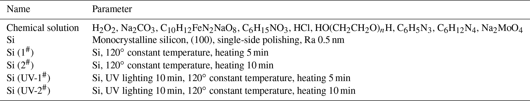
In order to study the effect of UV on the chemical modification of monocrystalline silicon, different modification strategies were designed and corresponding experimental results were discussed. A weak alkaline solution for monocrystalline silicon was prepared (initial pH ≈ 11) based on a Fenton reaction. The special chemical solution mainly contains a Fenton reagent, pH value regulators, alkaline liquid, and other components listed in Table 1 (Aida et al., 2012; Li et al., 2020; Zhou et al., 2014). All monocrystalline silicon samples were produced as a cube with dimensions of mm3, with one side polished. Firstly, the samples were cleaned using deionized water, acetone, and anhydrous ethanol in an ultrasonic cleaning machine and then dried. The cleaned samples were put into a corundum vessel with the self-made weak alkaline solution. Secondly, the vessel containing the samples and solution was placed in an oil bath with a constant temperature. The Si (1#) sample and Si (2#) sample had been heated for 5 and 10 min, respectively, with a constant temperature of 120∘, which was named the single heating chemical modification strategy (H-CM). A UV photocatalytic reaction experimental device was equipped with 10 UV lamps and a shield case whose UV light intensity was 265 µw cm−2 and whose wavelength was 254 nm. The Si (UV-1#) sample and Si (UV-2#) sample were irradiated for 10 min in the UV device. In the meantime, they were heated for a different time, which was named UVA-CM. These experimental details are shown in Table 1. The effects of heating time, UV lighting, and modification strategies on chemical modified efficiency are discussed.
Table 1The chemical modification strategy and experimental parameters.
3.2 Physical and chemical property tests
The amount of silicon deposited in different samples' reaction solutions was detected by inductively coupled plasma mass spectrometry (Spectroblue ICP-OES); the effect of different strategies on reaction rate was evaluated. The qualitatively functional groups of modified layers of samples were detected by using a confocal Raman microscope (WiTec Alpha300R), and the Raman spectroscopy characteristic peaks were compared to analyze the compositions of modified samples.
Nanoindentation and scratch tests were performed using a Berkovich indenter (Keysight Nano Indenter G200). The tip radius of the Berkovich indenter is 400 nm. To compare the thickness of modified layers of different samples, the maximum loads of 30 and 50 mN were applied, respectively. Each sample was tested five times. The nanohardness values were analyzed to evaluate the mechanical properties of the modified layer. A continuous scratch test with the constant speed was carried out with the loading range of 0–80 mN, loading speed of 4 mN s−1, indenter moving speed of 10 µm s−1, and scratch displacement of 20 µm. The scratch morphology was observed using an ultra-depth microscope (VH-Z100R) and atomic force microscopy (Veeco Multimode-V) to reveal the material removal mechanism.
4.1 Physical and chemical properties and morphology
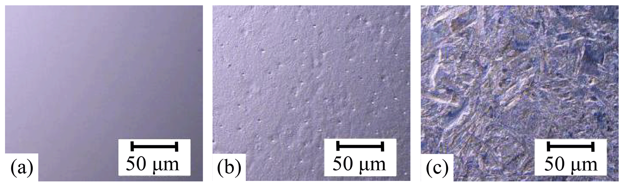
The surface morphology of the sample was observed with an ultra-depth microscope, as shown in Fig. 2. The Si sample shows a very smooth surface (Fig. 2a), but there were some pits with varying depths on the Si (2#) sample surface under the H-CM strategy (Fig. 2b). The Si (UV-2#) sample exhibited more mottled surface morphology, with a greater range of pits and a large crisp layer morphology (Fig. 2c). However, the distribution of the modified surface morphology was uniform regardless of pits or crisp layer. The chemical solutions of the Si (2#) and Si (UV-2#) samples were extracted for ICP detection. The amount of silicon deposited in the chemical solution of the Si (2#) and Si (UV-2#) samples was 337.7 and 667.2 mg L−1, respectively. It can be seen that the chemical reaction occurred between samples and chemical solution when using different modification strategies. When heated for the same time, the amount of silicon deposited in the chemical solution of the Si (UV-2#) sample was twice the one from Si (2#). It indicated that UV irradiation can accelerate the reaction rate at the same reaction temperature and enhance the efficiency of the chemical modified solution.
It is well known that the lifetime of •OH is extremely short in the Fenton reaction according to Eq. (1). However, UV light can trigger a reduction reaction focusing on products of the Fenton reagent according to advanced oxidation reaction. It contributes to transferring the oxidized Fe3+ into Fe2+ according to Eq. (8). Under UV irradiation, the recycling efficiency of Fe2+ was enhanced and then played the role of a cyclic catalytic effect to produce •OH. In the meanwhile, UV light further catalyzes H2O2 to generate •OH according to Eqs. (5)–(7). Under UV irradiation, the chemical modification solution continuously produced a higher concentration of •OH. Under the UVA-CM strategy, it not only extended the amount of •OH in the solution to a certain extent, but also prolonged the existence time of •OH in the solution.
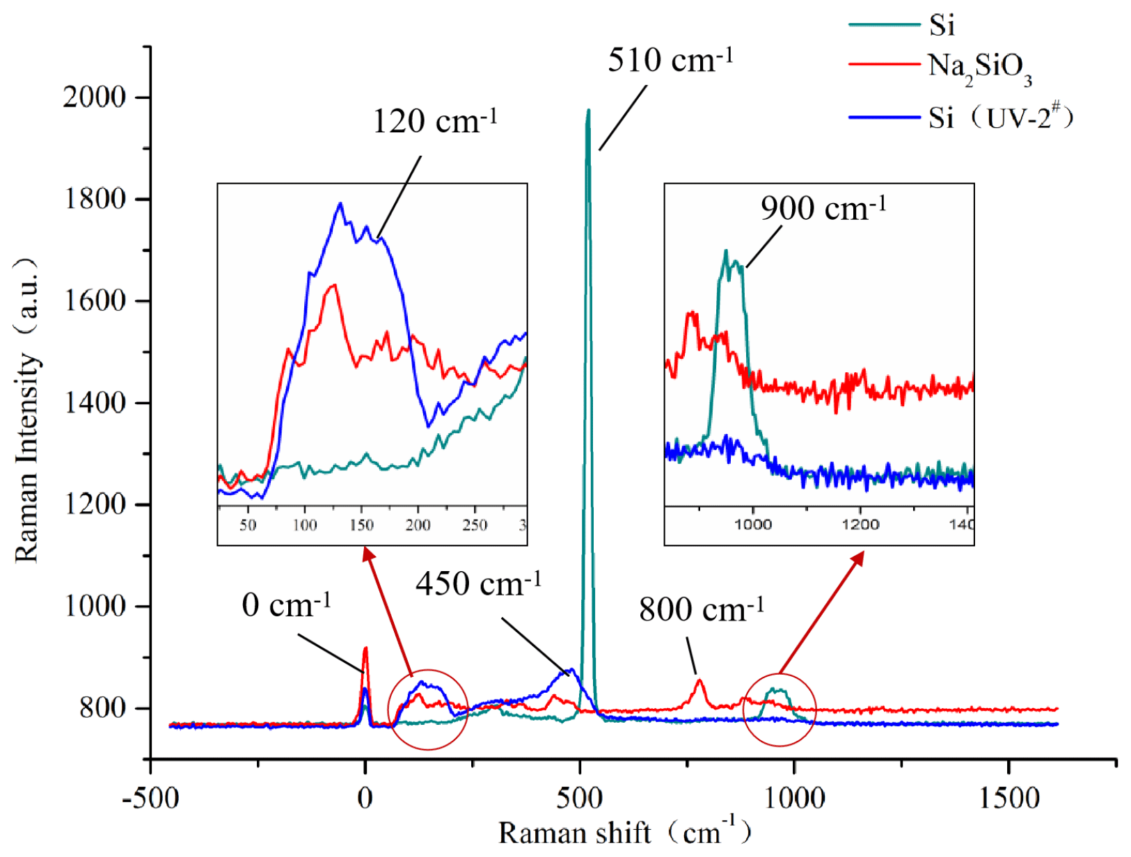
Comparing the Raman spectroscopy of the Si (UV-2#) and Si samples, the Si sample presented an obvious characteristic peak at a Raman shift of 510 cm−1 as shown in Fig. 3, but the Si (UV-2#) sample did not have the similar characteristic peak at this shift. It indicated that the Si–Si bond of the Si (UV-2#) surface was broken. There was a weaker peak presenting at a Raman shift of 900 cm−1 of the Si sample. It indicated that its surface contained other oxide impurities (Xu, 2014). As for the Si (UV-2#) sample, some peaks occurred at Raman shifts of 120 and 450 cm−1, which was similar to the analytical pure Na2SiO3 powder. Thus, some silicate was formed on the mottled surface of the Si (UV-2#) sample. It was demonstrated that the silicate layer could be created on the sample's surface under the UVA-CM strategy.
4.2 Nanoindentation analysis
The load–depth curve of nanoindentation is employed to analyze the mechanical behavior of samples under different strategies (Fig. 4). This curve can explain the variation trend of nanoindentation depth via load on the modified layer during loading and unloading. When the maximum load was 30 mN, the load–depth curves of Si, Si (1#), and Si (2#) almost coincided, as shown in Fig. 4a. At the holding stage of 30 mN, the maximum indentation depths of Si, Si (1#), and Si (2#) samples were nearly the same at 310 nm. However, the springback residual depth of Si was approximately 175 nm after unloading, which was slightly lower than that of Si (1#) and Si (2#). Even so, there were a certain number of chemical reactions happening between monocrystalline silicon and chemical solution under the H-CM strategy, but the fresh modified layer was extremely thin. Under the maximum loading of 30 mN, the difference of mechanical behavior among Si, Si (1#), and Si (2#) was very limited. It was obvious that the curves of Si (UV-1#) and Si (UV-2#) were fairly different from the Si sample under the UVA-CM strategy. At the holding stage, the maximum indentation depths of Si (UV-1#) and Si (UV-2#) were about 345 and 420 nm, respectively. In the unloading stage, the minimum springback residual depths of Si (UV-1#) and Si (UV-2#) were about 210 and 295 nm, respectively. The increase in springback residual depth indicated the increase in the degree of plastic deformation. It can be seen that the modified layer of Si (UV-2#) exhibited the largest thickness. Compared with the H-CM strategy, the UVA-CM strategy presented a higher chemical modification efficiency and a larger thickness modified layer. From the deepening of plastic deformation, it can be inferred that the maximum indentation depth of the indenter at 30 mN did not penetrate the modified layers of the Si (UV-1#) and Si (UV-2#) samples.

Figure 4The load–depth curve of nanoindentation samples of the (a) 30 mN load and the (b) 50 mN load.
When the load smoothly increased to 50 mN, in the holding stage the indentation depth of the Si (UV-2#) sample extended to 530 nm (Fig. 4b), which was obviously different from others. Excepting the Si (UV-2#) sample, nearly all samples' curves basically coincided. Under the maximum loading 50 mN, the Si (UV-1#) sample exhibited similar mechanical behaviors for Si, Si (1#), and Si (2#), with maximum indentation depths varying between 423 and 450 nm during the holding stage. The modified layer of the Si (UV-1#) sample might be punctured by the indenter. It can be inferred that the thicknesses of modified layers of Si (1#) and Si (2#) were less than 300 nm, and the thickness of the modified layer of Si (UV-1#) ranges from 350 to 450 nm. In the unloading stage, the minimum springback residual depth of Si (UV-2#) was around 340 nm, and the Si (UV-2#) sample exhibited the largest plastic deformation in the maximum indentation depth range. At about 50 mN, the indenter had not yet penetrated the modified layer of Si (UV-2#) with a thickness of more than 520 nm. The test results showed that a deeper modified layer can be successfully obtained by introducing UV irradiation and extending the heating time of chemical modification.
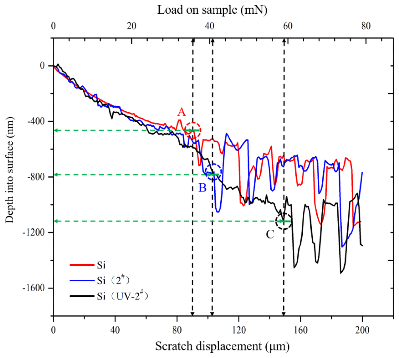
Figure 5The scratch displacement–depth–load curve of the Si, Si (2#), and Si (UV-2#) samples.
4.3 Scratch analysis
Figure 5 shows the relationship among the scratch displacement, scratch depth into surface, and load on sample. When the scratch load was below 10 mN, no apparent deformation occurred on all samples. The indenter displacement–depth–load curves of all samples basically coincide. Overall, in the range of 10–30 mN, the scratch displacement–depth–load curve of Si was relatively smooth, and the curves of Si (2#) and Si (UV-2#) fluctuated slightly in the scratch displacement direction. It can be explained that both surface roughness values of the Si (UV-2#) and Si (2#) samples were both larger than that of the Si sample because of the tiny pits and mottled areas on the modified layer surface as shown in Fig. 2b and c. When increasing loading to 36 mN, the scratch displacement–depth–load curve of the Si sample suddenly appears as a step-type drop at the depth of 400 nm, as shown at point A of the Si sample's curve in Fig. 5. Similarly, the Si (2#) sample's curve also appeared as a step-type drop at point B with a load of 41 mN and a depth of about 800 nm. Up to a load of 60 mN, the curve of the Si (UV-2#) sample showed a step-type drop at point C and a depth of about 1100 nm. When scratch displacement exceeded these step-type drops, these displacement–depth–load curves revealed more drastic oscillations with the indenter moving and load increasing. The displacement–depth–load curves of the Si and Si (2#) samples had similar oscillations and trends in the direction of scratch depth. When the load exceeded 60 mN, the Si (UV-2#) sample's displacement–depth–load curve also appeared fluctuation characteristic. Compared with others, its oscillations and interval trends were gradually similar to the Si sample's. It was inferred that brittle fracture behavior occurs at these step-type drop points. The step-type drop point was the critical transfer point for different material-removing models. Thus, the Si (UV-2#) sample occurred a brittle fracture at point C.
The transition interval between the modified layer and raw material layer probably appeared under the depth of 1120 nm (loading of 60 mN). At 60 mN load, the Si (UV-2#) sample's curve described a layered composite material characteristic, which is made up of the upper modified layer and the lower monocrystalline silicon layer. Beyond the 60 mN load, the scratch indenter contacted the monocrystalline silicon layer below the modified layer. Thus, the fluctuation characteristics in the depth direction of the curve were similar to that of the Si sample. The thickness of the modified layer of Si (UV-2#) may be beyond 520 nm while it was below 1120 nm.
Compared with the scratch morphology of the Si and Si (UV-2#) samples (Fig. 6), it can be clearly seen that both sides of scratches are smooth before the occurrence of lateral cracks. Since the sample has a certain elastic deformation region, it is difficult to determine the starting point of a scratch. From a scratch ending location according to indenter moving speed and microscopic scale, scratch displacement and load have been marked in the scratching microscopic morphology graph (Fig. 6). As for the Si sample's scratch, the first lateral crack propagation appeared approximately at a 90 µm location (point A in Fig. 6a), where the load was 36 mN, coinciding with point A in Fig. 5. The propagation length of the lateral crack extension scratch was about 5 µm. Taking point A in Fig. 6a as a characteristic point, the scratch morphology of the Si sample can be divided into three regions. The right-hand side of point A is defined as region III, which covers dense lateral cracks. The left-hand side of point A is regarded as the smooth region II, where it is difficult to find surface cracks. However, the initial scratch point and the elastic deformation region I cannot be directly determined in the microscopic picture as there is no obvious scratch. Due to a total scratch displacement of 200 µm, backward reasoning measurement had been adopted to mark the initial scratch point and the elastic deformation region I based on ending location. Moreover, for the Si sample in region II, the surfaces of scratch sides appeared smooth, and the width of the scratch varies from narrow to wide, which showed typical plastic removal characteristics (Fig. 6a). In region III, typical lateral cracks appeared on both sides of the scratch with the increase in displacement and load, which showed typical brittle fracture removal characteristics (Fig. 6a). With increasing displacement and load, the space of the lateral crack became more and more dense. The crack propagation length became much longer. The phenomenon was consistent with the fluctuation trend of the displacement–depth–load curve of the Si sample as shown in Fig. 5.
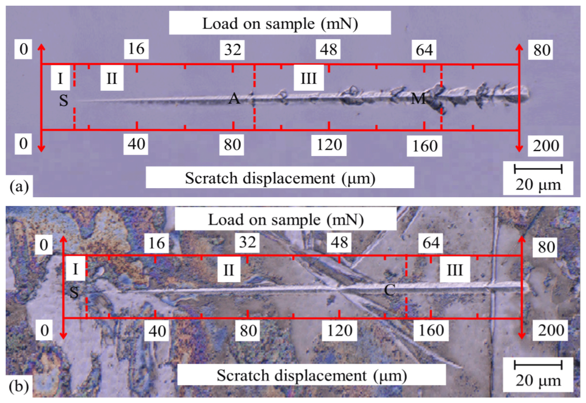
Compared with the Si (UV-2#) sample, although the Si (UV-2#) sample surface presented obvious spots due to UVA-CM, both sides of the scratch were smooth and integrated. No significant lateral crack propagation was observed at current magnification (Fig. 6b). According to fluctuation characteristics of the Si (UV-2#) sample's curve shown in Fig. 5, the brittle fracture phenomenon occurs when scratch load goes beyond 60 mN. Perhaps these details of the lateral crack were covered up because of a mottled modified layer under insufficient magnification in Fig. 6b. Similarly, the scratch morphology of the Si (UV-2#) sample can also be divided into three regions. Taking point C in Fig. 5 as a characteristic point, according to the indenter, moving speed and microscopic scale at point C in Fig. 6b were marked. Although no obvious lateral crack was found in point C under current magnification of Fig. 6b, the brittle fractures probably caused crack nucleation below the surface. The left-hand side of point C of the smooth and crack-free region was named region II. The right-hand side of point C to the scratch end was named region III (Fig. 6b). Region I without an obvious scratch was estimated according to the total scratch displacement.
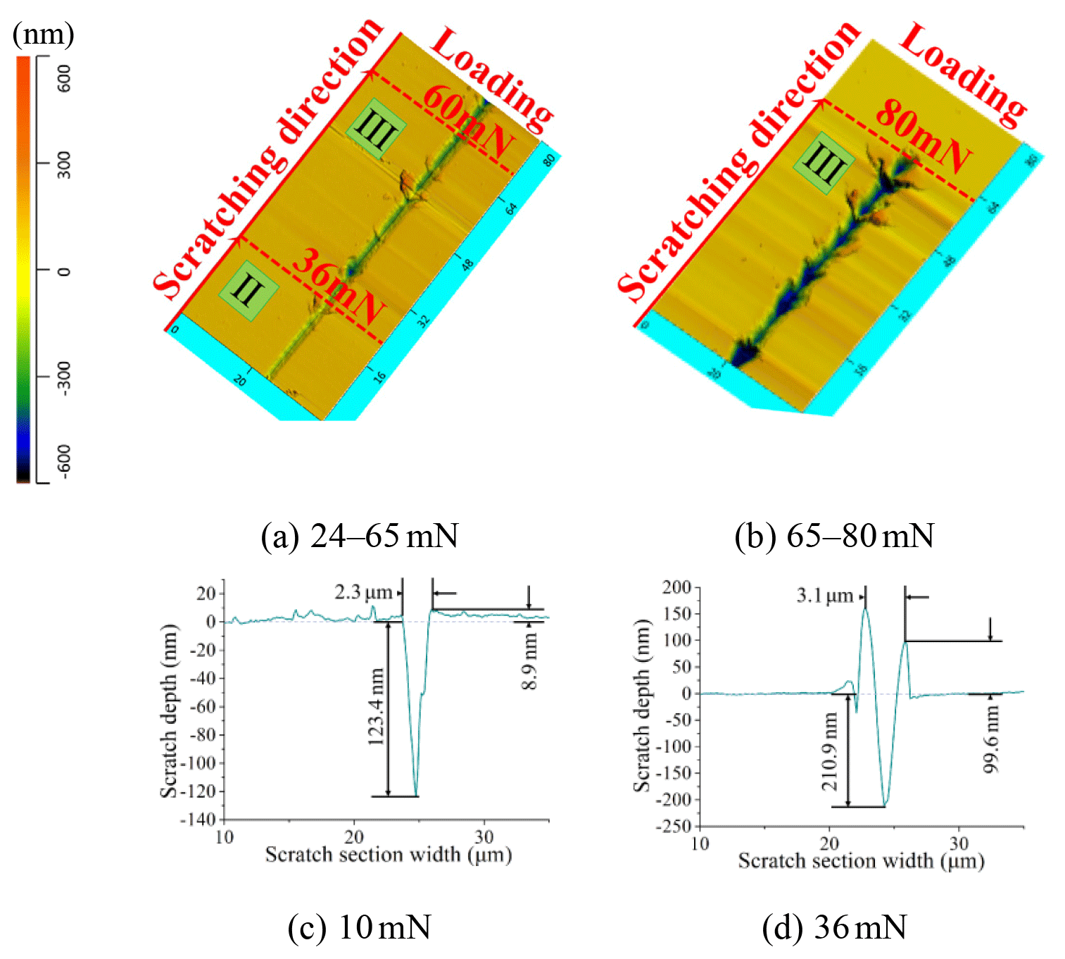
The typical scratch surface and section morphology were observed by atomic force microscopy (AFM), as shown in Figs. 7 and 8. In Fig. 7a, there were about five lateral cracks extending to the surface which basically correspond to these fluctuant positions on the scratch displacement–depth–load curve of Si in the load range of 30–60 mN in Fig. 5. It was further explained that the fluctuant position on the scratch displacement–depth–load curve behaves like the brittle fracture phenomenon. With increased displacement and load, the removal characteristics of brittle fracture became more obvious, and the size of the crack propagation became much larger (Fig. 7b). Before the first lateral crack propagation, the scratch section morphology presented typical plastic removal characteristics. For example, at the load position of 10 mN, the section profile of the scratch displayed a V shape according to the Berkovich indenter. There were some pile-ups around the side of the scratch (Fig. 7c). The residual depth was 124 nm, the residual width was 2.3 µm, and the height of pile-ups was 9 nm. In the load range of 30–60 mN, the Si sample exhibited both plastic and brittle fracture removal characteristics.
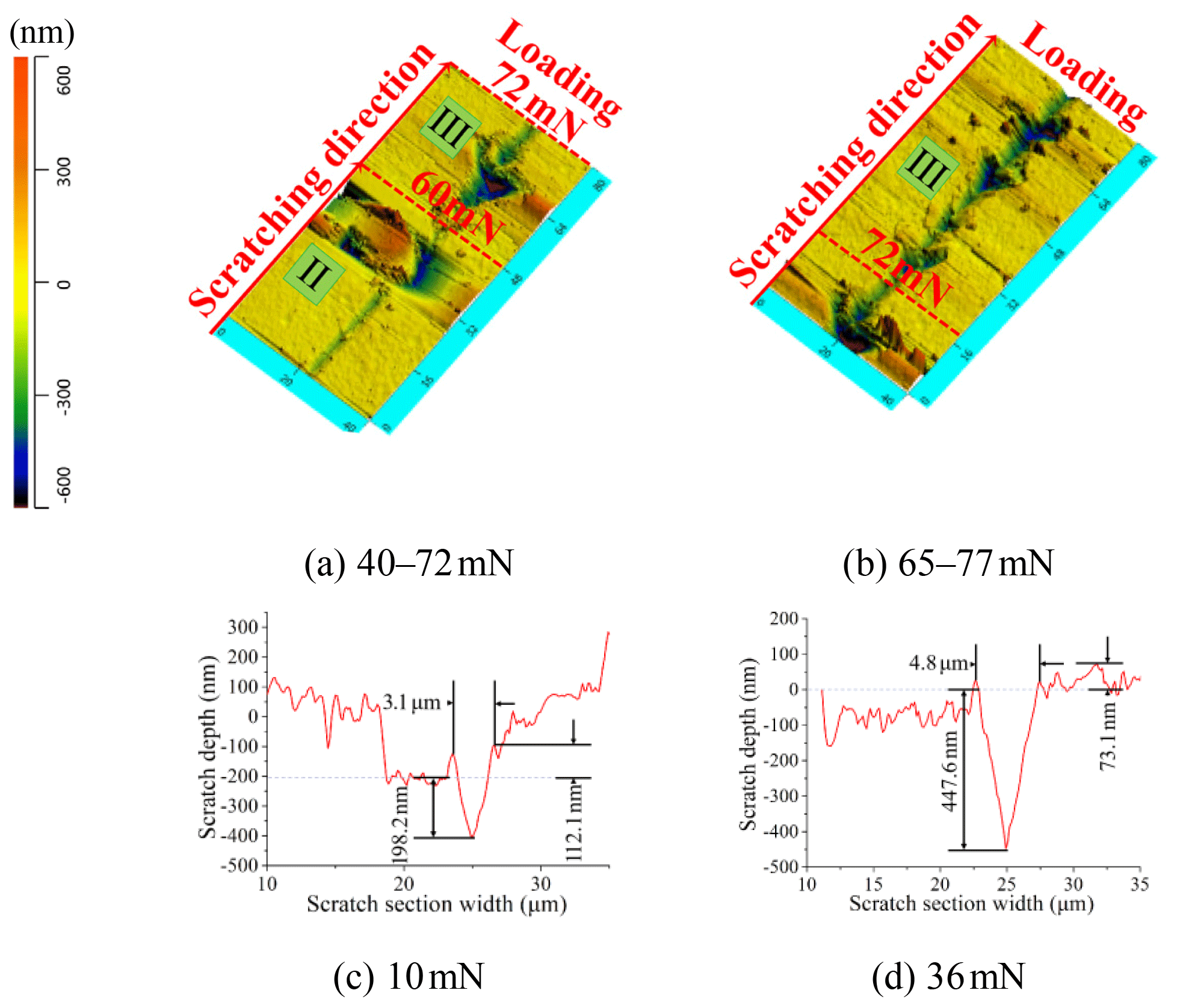
Compared to Figs. 7 and 8, in the same load and displacement range, the Si (UV-2#) sample showed a longer displacement plastic deformation region and a smaller crack propagation size than the Si sample (Fig. 8). Lateral crack propagation occurred when the load exceeded 60 mN (Fig. 8a). The scratch section profile of the Si (UV-2#) sample also formed a V shape at 10 mN (Fig. 8c), although the residual widths were almost the same in Figs. 7c and 8c, which were 2.3 and 3.1 µm, respectively. However, its residual depth was 198 nm and the height of the pile-up was 112 nm, both exceeding the one observed on the Si sample under 10 mN load. Especially under 36 mN load the section scratch profile of the Si (UV-2#) sample exhibited almost twice the residual depth as that of the Si sample as shown in Fig. 8d. It is demonstrated that under the UVA-CM strategy the modified layer of the Si (UV-2#) sample exhibited more plastic material removal than the raw material of the Si sample. In addition, the number of cracks in the load range of 40–72 mN in Fig. 8b was consistent with the number of fluctuant positions within the same range of the Si (UV-2#) sample in Fig. 5. It indicated that the chemical modification contributes to inhibiting crack nucleation and propagation. Due to the chemical modification, the sample surface became a composite structure of low-hardness silicate layer and high-hardness monocrystalline silicon substrate layer. Lateral cracks nucleated in the high-hardness monocrystalline silicon substrate layer and propagated in the low-hardness silicate layer. Consequently, under the same scratch condition, the Si and Si (UV-2#) samples presented obviously different positions of lateral crack nucleation and propagation degree.
According to the experimental results of nanoindentation and scratch, with only single assisted heating, the reaction rate of the Fenton reagent is limited. The thickness in nanometers of the modified layer was produced, with a slight difference in mechanical properties under the H-CM strategy. The UV photocatalysis contributes to improving the modification efficiency of the chemical modification solution and accelerates the reaction rate by inputting more energy. According to Eqs. (5)–(8), based on the principle of UV advanced oxidation reaction, the recycling efficiency of •OH in the chemical modified solution was significantly improved. Therefore, compared with the H-CM strategy, the UVA-CM strategy can facilitate chemical modification of monocrystalline silicon in a short time. The modified samples presented layered structures with lower hardness, which was very beneficial for restraining the crack propagation. Generally, during the micro-machining of monocrystalline silicon micro-structures, such as micro-grinding, the undeformed cutting thickness of a single abrasive should be around 200 nm to achieve ductile removal (Muhammad et al., 2013). According to the controlling modification strategy a workpiece surface can form a modified layer with a certain thickness and lower hardness, for example the modified layer thickness of the Si (UV-2#) sample being in the range of 520–1100 nm. The chemical modified layer thickness greatly exceeded the undeformed cutting thickness of a single abrasive for monocrystalline silicon. Therefore, when introducing the UVA-CM strategy into monocrystalline silicon micro-grinding in future applications, the mechanical removal process might become easier, and the processing quality and efficiency could also be improved. Hence, the UVA-CM strategy will contribute to developing a novel chemo-mechanical processing technology for machining monocrystalline silicon.
This article aims to develop a UVA-CM strategy to improve chemical modification efficiency and modify mechanical properties of monocrystalline silicon. The comparative experiments were designed. The chemical and mechanical properties of the modified samples were tested and analyzed. The following main conclusions can be drawn as follows.
-
Under the same chemical solution environment, the UVA-CM strategy can produce a faster modification rate and a lower hardness of the modified layer compared with the performance of the H-CM strategy.
-
Under the UVA-CM strategy, the nanohardness of the modified layer is significantly decreased for monocrystalline silicon. However, the hardness distribution is uneven due to the mottled modified layer morphology.
-
Under the UVA-CM strategy, the modified sample has a composited layer structure, with a modified layer thickness of 520–1100 nm. The modified layer can effectively inhibit lateral crack nucleation and propagation under a certain scratch depth. The UVA-CM strategy is recommended for developing a novel chemo-mechanical technology for micro-grinding of monocrystalline silicon.
The data generated during this study are available from the corresponding author on reasonable request.
YR contributed to this work by proposing the principle design of the UVA-CM strategy and establishing a comparative experiment. KL contributed to manuscript writing and data collection and analysis. WL contributed to the guidance of the experiment. XH and XL contributed to carrying out experiment research.
The authors declare that they have no conflict of interest.
This article is part of the special issue “Robotics and advanced manufacturing”. It is not associated with a conference.
We thank Huigao Duan and Maojun Li (Hunan University) for their assistance in chemical property testing. Moreover, we thank the National Natural Science Foundation of China for the financial supports.
This research has been supported by the National Natural Science Foundation of China (grant nos. 51675170, 52075161, and 51875192).
This paper was edited by Peng Li and reviewed by Bing Guo and one anonymous referee.
Aida, H., Doi, T., Takeda, H., Katakura, H., Kim, S. W., Koyama, K., Yamazaki, Y., and Uneda, M.: Ultraprecision CMP for sapphire, GaN, and SiC for advanced optoelectronics materials, Curr. Appl. Phys., 12, 41–46, https://doi.org/10.1016/j.cap.2012.02.016, 2012.
Alamgir, A., Bogatov, A., Yashin, M., and Podgursky, V.: Mechanical and tribological properties of 100-nm thick alumina films prepared by atomic layer deposition on Si(100) substrates, P. Est. Acad. Sci., 68, 126–130, https://doi.org/10.3176/proc.2019.2.01, 2019.
Aurich, J. C., Carrella, M., and Walk, M.: Micro grinding with ultra-small micro pencil grinding tools using an integrated machine tool, CIRP Ann-Manuf. Techn., 64, 325–328, https://doi.org/10.1016/j.cirp.2015.04.011, 2015.
Aurich, J. C., Kirsch, B., Setti, D., Axinte, D., and Yamaguchi, H.: Abrasive processes for micro parts and structures, CIRP Ann-Manuf. Techn., 68, 653–676, https://doi.org/10.1016/j.cirp.2019.05.006, 2019.
Ishimarua, D., Tougea, M., Mutaa, H., Kubotaa, A., Sakamoto, T., and Sakamoto, S.: Burr Suppression Using Sharpened Pcd Cutting Edge by Ultraviolet-Ray Irradiation Assisted Polishing, Procedia CIRP, 1, 184–189, https://doi.org/10.1016/j.procir.2012.04.032, 2012.
Kubota, A., Kurihara, K., and Touge, M.: Fabrication of Smooth Surface on 4H-SiC Substrate by Ultraviolet Assisted Local Polishing in Hydrogen Peroxide Solution, Key Eng. Mater., 523, 24–28, 2012a.
Kubota, A., Yoshimura, M., Fukuyama, S., Iwamoto, C., and Touge, M.: Planarization of C-face 4H-SiC substrate using Fe particles and hydrogen peroxide solution, Precis. Eng., 36, 137–140, https://doi.org/10.1016/j.precisioneng.2011.09.003, 2012b.
Li, C., Zhang, F. H., Meng, B. B., Liu, L. F., and Rao, X. S.: Material removal mechanism and grinding force modelling of ultrasonic vibration assisted grinding for SiC ceramics, Ceram. Int., 43, 2981–2993, https://doi.org/10.1016/j.ceramint.2016.11.066, 2017.
Li, W., Chen, Q. D., Ren, Y. H., Jiao, Y., and Ibrahim, A. M. M.: Hybrid micro-grinding process for manufacturing meso/micro-structures on monocrystalline silicon, Mater. Manuf. Process, 36, 17–26, https://doi.org/10.1080/10426914.2020.1813890, 2020.
Lu, C., Qiu, Z. J., Yi, P., and Yang, X.: Trial Production of Special Grinding Fluid for Efficient and Precise Quartz Glass Grinding, J. Mater. Sci. Eng., 31, 794–798, https://doi.org/10.14136/j.cnki.issn1673-2812.2013.06.012, 2013.
Lu, J. B., Chen, R., Liang H. Z., and Yan Q. S.: The influence of concentration of hydroxyl radical on the chemical mechanical polishing of SiC wafer based on the Fenton reaction, Precis. Eng., 52, 221–226, https://doi.org/10.1016/j.precisioneng.2017.12.011, 2017.
Muhammad, A., Zhang, X. Q., Mustafizur, R., and Kumar, S.: A predictive model of the critical undeformed chip thickness for ductile-brittle transition in nano-machining of brittle materials, Int. J. Mach. Tool Manu., 64, 114–122, https://doi.org/10.1016/j.ijmachtools.2012.08.005, 2013.
Qiu, Z. J., Zhou, L. B., Fang, F. Z., Shina, T., and EDA, H.: Chemical mechanical grinding for quartz glass, Optics Precis. Eng., 18, 1554–1561, https://doi.org/10.3788/OPE.20101807.1554, 2010.
Qiu, Z. J., Yi, P., Lu, C., and Fang, F. Z.: Mechanical Property Analysis of Modified Quartz Glass, J. Mater. Sci. Eng., 31, 6–10, https://doi.org/10.14136/j.cnki.issn1673-2812.2013.01.015, 2013.
Xu, M.: A spectroscopic study on the decomposition of magnesium silicate by alkali fusion using NaOH, PhD thesis, Northeastern University, Shenyang, 132 pp., 2014.
Ye, Z. F., Zhou, Y., Xu, L., and Pan, G. S.: Chemical mechanical polishing of 4H-SiC wafer with UV-LED light, Nanotechnol. Precis. Eng., 15, 342–346, https://doi.org/10.13494/j.npe.20170005, 2017.
Yuan, J. L., Zhang, F. H., Dai, Y. F., Kang, R. K., Yang, H., and Lv, B. H.: Development Research of Science and Technologies in Ultra-precision Machining Field, J. Mech. Eng., 46, 161–177, https://doi.org/10.3901/JME.2010.15.161, 2010.
Zhang, N. D., Zheng, W., Huang, J. L.: The application of UV-Vis/H2O2/ferrioxalate in wastewater treatment, Photographic Sci. Photoch., 21, 72–78, https://doi.org/10.7517/j.issn.1674-0475.2003.01.72, 2003.
Zhou, L. B., Shiina, T., Qiu, Z. J., Shimizu, J., Yamamoto, T., and Tashiro, T.: Research on chemo-mechanical grinding of large size quartz glass substrate, Precis. Eng., 33, 499–504, https://doi.org/10.1016/j.precisioneng.2009.01.006, 2009.
Zhou, Y., Pan, G. S., Shi, X. L., Gong, H., Luo, G. H., and Gu, Z. H.: Chemical mechanical planarization (CMP) of on-axis Si-face SiC wafer using catalyst nanoparticles in slurry, Surf. Coat. Tech., 251, 48–55, https://doi.org/10.1016/j.surfcoat.2014.03.044, 2014.