the Creative Commons Attribution 4.0 License.
the Creative Commons Attribution 4.0 License.
 | 27 Apr 2021
Simulation and fabrication of carbon nanotube–nanoparticle interconnected structures
Xiwen Lu
Jinhang Liu
Ye Ding
Lijun Yang
Zhan Yang
Yang Wang
With the rapid development of nanotechnology, the size of a device reaches sub-nanometer scale. The larger resistivity of interconnect leads to serious overheating of integrated circuits. Silicon-based electronic devices have also reached the physical limits of their development. The use of carbon nanotubes instead of traditional wires has become a new solution for connecting nano-structures. Nanocluster particles serving as brazing material play an important role in stabilizing the connection of carbon nanotubes, which places higher demands for nanoscale manipulation techniques. In this paper, the dynamic processes under different operating scenarios were simulated and analyzed, including probe propulsion nanoparticle operation, probe pickup nanoparticle operation and probe pickup nanocluster particle operation. Then, the SEM (Scanning Electron Microscope) was used for nanoparticle manipulation experiments. The smallest unit of carbon nanotube wire was obtained by three-dimensional (3D) construction of a carbon nanotube–silver nanocluster particle (CN-AgNP), which verified the feasibility of 3D manipulation of carbon nanotube wire construction. The experiments on the construction of carbon nanotube–nanocluster particle structures in three-dimensional operation were completed, and the smallest unit of carbon nanotube wire was constructed. This nano-fabrication technology will provide an efficient and mature technical means in the field of nano-interconnection.
- Article
(1075 KB) - Full-text XML
- BibTeX
- EndNote


Nanoparticle manipulation technology plays a crucial role in driving multifunctional integration and microstructuring in nanomanufacturing. Every breakthrough in nanoparticle manipulation technology can trigger revolutionary advances in nanomanufacturing (Stergar and Osterman, 2020; Komissarenko et al., 2020; Conradi et al., 2020; Shu et al., 2019). Small-sized nanoelectronic devices are greatly affected by quantum effects. Traditional semiconductor principles cannot explain this phenomenon. In recent years, scientists have proposed a method of using carbon nanotubes instead of existing wires to achieve the functionality of connected nanodevices (Mohsin et al., 2013; Bocko et al., 2018; Robinson and Adali, 2019). Carbon nanotube wires can be used to connect microelectrodes and macroscopic devices owing to their excellent electrical conductivity and microscopic properties, which can build the construction of cross-scale systems to satisfy the high-sensitivity and high-performance functions required in the fields of biology and information (Wang et al., 2013; Yuan et al., 2018; Bocko and Lengvarský, 2017). These new electronic devices are still in the stage of experimentation and exploration, and the connection method of carbon nanotube wires is still a problem to be solved.
In 2003, Fukuda developed a nano-operating platform system with 16 degrees of freedom integrated with four operating units (Fukuda et al., 2003; Yang et al., 2016; Shi et al., 2017), which is capable of realizing nanoscale- to millimeter-scale step motion and measuring the electrical properties (Yu et al., 2017a) and physical properties such as Young's modulus (Fukuda et al., 2005) of carbon nanotube materials as well as controlling the construction of complex nanostructures in three dimensions (Yu et al., 2017b). Zhang et al. (2011) developed a new positioning device to help positioning in nano-operation. The pickup and bend processes of one-dimensional zinc oxide material under the experimental platform are carried out successfully. Bartenwerfer and Fatikow (2012) implemented the technique of autofocusing in nano-operation and successfully performed experiments on picking up CNT and placing it on the substrate. Ru et al. (2010) developed an SEM operating platform, which is capable of coordinating four operating units that can perform complex testing and operational tasks. Williams et al. (2002) combined AFM and SEM to construct a system with excellent operating and visualization performance and conducted experiments on the operation of nanowires. Zimmermann et al. (2014) used an electron etch-shaped tungsten probe with a high aspect ratio and pocket shape as an end-effector to realize the clamping, placement and assembly of nanoparticles. The principles of large contact area and high adsorption force are used to fully utilize the probe and material adsorption force for efficient operation.
The SEM nano-operating platform is suitable for the operation of nanoclusters, but the current research on the operation of nanoparticles based on the SEM platform is mainly focused on the two-dimensional operation such as pushing and pulling. There is less research on the three-dimensional cross-substrate operation, and the forces on nanoparticles and nanoclusters during the operation are still unclear. In this paper, we use nanoscale manipulation techniques to control the silver nanocluster particles that serve as the brazing material for carbon nanotube connections. A CN-AgNP structure is constructed through three-dimensional manipulation across scales, which can serve as the basic unit for carbon nanotube conductors and provide a basis for carbon nanocluster interconnection technology. Unlike the current two-dimensional push–pull operation, the three-dimensional operation can build independent single carbon nanotube connection structures on empty substrates, which avoids situations where the electrical properties of the substrate are affected due to the dispersion of particles on the substrate. Since the three-dimensional operation of nanoparticles, nanocluster particles especially have not been deeply studied and the absorption mechanism of nanoparticles and nanocluster particles is still unclear, this article provides new ideas for the interconnection and nanomanipulation of carbon nanotubes.

2.1 The probe drives silver nanoparticles
The Maugis–Dugdale (M–D) model (Maugis, 1992) is a synthesis of the Johnson, Kendall and Roberts (JKR) model and the Derjaguin, Muller and Toporov (DMT) model. By introducing a dimensionless Tabor, the adhesion phenomenon and the van der Waals force outside the contact surface are integrated. The M–D theory's description of the contact situation of nano-scale objects can meet the needs of this research, so the force model is built based on the M–D contact theory. As shown in Fig. 1, P1 is the Hertz pressure acting on the contact surface, and P2 is the adhesive force acting on the radius c, where the contact force is
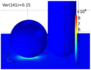
According to the M–D model, the simulation results are shown in Fig. 2. During nano-operation, the movement of nanoparticles is often achieved by pushing the nanoparticles on the substrate plane by means of a probe. This operation brings the probe close to one side of the nanoparticle and applies a constant pushing force to the probe in the horizontal direction to control sliding. During the operation, the nanoparticles are subjected to contact and frictional forces of the substrate as well as the contact and thrust forces of the probe. The contact force between nanoparticles and substrate remains unchanged. Then the friction force gradually increases from zero. The thrust between nanoparticle and substrate remains unchanged, and the contact force increase with increasing of the relative displacement. When the nanoparticle overcomes the maximum static friction, the contact force remains unchanged.
After analyzing the process of probe propulsion of the nanoparticles, a model describing the probe propulsion of silver nanoparticles on SiO2 substrate was built according to the operational process. COMSOL is used to study the steady state of solid mechanics modules of the selected type. The nanoparticles are placed on the substrate. The probe is placed at one side of nanoparticles. The side wall of the probe is perpendicular to the x axis. The radius of curvature of probe tip R0 is 30 nm, the radius of the nanoparticles R1 is 40 nm, and the length, width and height of the substrate are set as 400, 400, and 100 nm, respectively. The probe material is Au. The nanoparticle material is Ag. The substrate material is SiO2. The contact pairs of probe–nanoparticle and nanoparticle–substrate are established and set the adhesion and peeling conditions between the contact pairs. The outside surface of basilar is constrained to establish the integral function of the opposite surface.
It can be observed that there is a contact stress between nanoparticles and substrate before the probe contacts the silver nanoparticles. When the silver nanoparticles is pushed by the probe, the silver nanoparticles are moved, and the contact surface between probe and substrate generates a force. The magnitude of the force is equal to the friction between the nanoparticles and the substrate, and it is smaller than the contact force between the silver nanoparticles and the substrate.
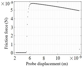
The frictional curve is shown in Fig. 3. When the relative displacement is 5 nm, the contact stress is generated between the probe and nanoparticle. The friction of the nanoparticle rises rapidly from zero to the maximum static friction. After that, the silver nanoparticle is pushed by the probe, and the friction gradually decreases. When the friction decreases to the sliding friction, the friction is unchanged.
2.2 Probe picks up silver nanoparticles
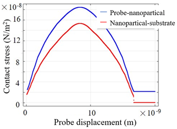
Nanomanipulation not only requires two-dimensional push operations in the plane of the substrate, but also requires the application of spatial three-dimensional operation methods when building complex systems. Therefore, the study of the three-dimensional picking operation process is necessary. The operation of the probe picking up silver nanoparticles is studied, and the picking process obtained by simulation is shown in Fig. 4. Initially, there is a contact force between probe and nanoparticle. The material is deformed in the process of pressing the probe, and the stress between the contact surfaces increases significantly with the relative displacement. In the process of lifting, adhesion occurs between probe and nanoparticle, and peeling occurs between the nanoparticle and the substrate. Finally, the nanoparticle is separated from the substrate with the probe to complete the pickup operation.

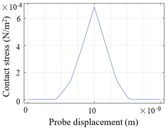
Figure 5 shows the change in contact stress with probe displacement during the process of picking up nanoparticles. It can be seen that the nanoparticles elastically deform with the probe pressing down, and the stress between the contact surfaces gradually increases. Because the material and the shape are different, the distribution of stress will be different. Although the net force of the two contact surfaces is equal, their maximum stress is not entirely equal. It is divided into three stages in the process of the probe lifting. The first stage is the contact state between the probe and nanoparticle and the nanoparticle and substrate. As the elastic deformation of the material recovers, the contact force decreases rapidly. In the second stage, the two contact pairs are in an attractive state. The contact force gradually decreases with the change in distance from the repulsive force and then turns into gravitational force. In the third stage, a nanoparticle is picked up by the probe and detached from the substrate. The probe and nanoparticle are still in an attractive state, and the interaction force remains unchanged. Nanoparticle and substrate are in a separated state, and the interaction force can be ignored.
2.3 The probe picks up nanocluster particles
The simulation results are shown in Fig. 6. The nanocluster model is built as a tetrahedral structure consisting of four nanoparticles of the same radius to simulate the process of picking up nanocluster particles from the substrate by an analytical probe. It can be found that the probe is able to stabilize the pickup of the nanocluster particles so that they can detach from the substrate. The four single nanoparticles that make up the nanocluster particles undergo relative motion during the pickup process. When the probe is pressed down, the three nanoparticles at the bottom show a tendency to separate outwardly. The particles at the top move down relative to the other three particles, and the overall shape of the nanocluster particles becomes wider and flatter. In the lifting stage of the probe, the nanocluster particles are pulled and the overall shape is elongated. The nanoparticles are deformed by adhesion. The relative positions of the three nanoparticles at the bottom become closer, and the nanoparticles at the top are farther away from the plane where the three nanoparticles at the bottom are located. When the nanocluster particles leave the base, the force between the nanocluster particles and the base is almost zero, and there is contact force between the nanocluster particles and the probe. Because the distance between the nanocluster particles and the probe remains the same, the contact force between nanocluster particles and probe is unchanged.
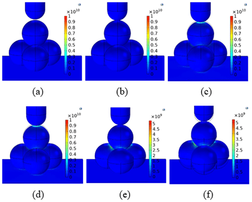
Figure 6Process diagram of probe pickup of nanoclusters. (a) Initial state, (b) probe contacts with nanoparticles, (c) probe is moving down, (d) probe contacts with the bottom, (e) probe is moving up, and (f) nanoparticles detach from the substrate.
Figure 7 shows the curve of the force between nanocluster particles and substrate. When the probe is in the same relative displacement, the contact stress during the downforce process is greater than that during the uplift process. This is due to the adhesion effect between the nanocluster particles and the substrate after the downward pressure. When the probe is lifted, the nanocluster particles will give an additional upward adhesion to the substrate, resulting in a lower contact stress than that under the downward pressure.
Simulation results show that the contact stress exists between nanoparticle and probe and nanoparticle and substrate during the pushing operation. The friction between nanoparticles and substrate increases gradually. When the maximum static friction force is reached, the nanoparticle begins to slide, and the friction force gradually decreases to sliding friction force and finally remains unchanged. The probe can pick up silver nanoparticles and silver nanoparticle clusters on the SiO2 substrate during the pickup operation. The adhesion and peeling phenomenon occurs between the nanoparticles and the substrate at the contact stage. After separating from the base, the force between nanoparticles and nanocluster particles and the basement is almost zero, and there is still a strong adhesive contact force between the probe and the nanoparticle. The nanoparticles that constitute the nanocluster remain in the state of binding, which can realize the stable picking operation of the nanoparticles and the nanocluster.
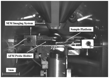
This experiment is carried out on the nanometer operating system under SEM, which has the characteristics of real-time observation, efficient nanometer manipulation and accurate position positioning. The AFM probe and the dispersed sample are fixed on a clamping device and the sample clamping device, respectively, as shown in Fig. 8.
The three-dimensional (3D) relocation of silver nanoclusters across the substrate can be achieved through three-dimensional picking up. Silver nanoclusters are picked up by the AFM probe to build the structure of carbon nanotube–silver nanoclusters. Silver nanocluster particles of suitable size on the ITO conductive glass substrate are selected. The silver nanocluster particles are adsorbed on the tip of the AFM probe free from the substrate confinement, and then the probe is moved to the end point of the scattered single carbon nanotube.
In the experiment, it was observed that the AFM probe can only adhere to the smaller silver nanocluster particles during operation. When adsorbing the larger silver nanocluster particles, some particles will separate from the cluster, taking into account that silver nanocluster particles are used as solder for interconnecting carbon nanotubes. The small size of the nanocluster particles may not be able to achieve the function of stable interconnection between carbon nanotubes. Therefore, the best results can be obtained by selecting silver cluster particles with a diameter of about 209.3 nm.
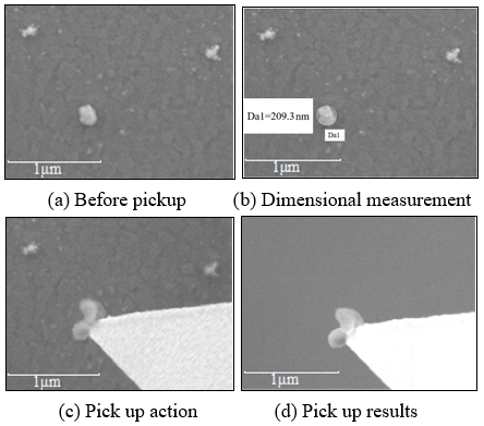
After selecting suitable silver nanocluster particles, three-dimensional pickup and relocation of the carbon nanotube–silver nanocluster particles were carried out; the steps are as follows.
-
Gradually and slowly descending the AFM probe through the Smart Act controller until the AFM probe tip is in the same plane as the substrate surface, at which point the AFM probe can manipulate the silver nanocluster particles on the substrate.
-
The AFM probe is used to increase the contact area with silver nanoclusters by pushing and pulling to pick up the nanocluster particles in three dimensions. It is observed that due to the large size of the selected nanocluster particles, the nanocluster is deformed and separated into two parts during the pickup process, and the AFM probe could not pick up the particles at once, so the remaining parts of the particles continued to adhere by pushing and pulling with the AFM probe, and due to the increased contact area, the nanocluster particles could adhere steadily to the AFM probe. The AFM probe is lifted off the substrate, and the three-dimensional pickup of silver nanocluster particles is completed, as shown in Fig. 9.
-
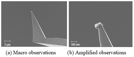
In order to observe the adhesion state of the AFM probe to silver nanocluster particles, the probe is lifted from the substrate, the probe through the SmarACT controller rotated, the magnification reduced, and it can be observed that the probe tips out of the silver nanocluster particle adhesion position, as shown in Fig. 10. At this time, the silver nanocluster particles are adhered to the side of the tip of the AFM probe, and they are flush with the tip of the probe in the vertical direction. Therefore, it is difficult to remove the silver nanocluster particles from the AFM probe by means of scratching or rubbing. The force of the end of the carbon nanotube on the silver nanoparticle should be used to place the silver nanoparticle at the target position.
-
The probe of the adhered nanocluster particles is rotated to the initial state, the AFM probe is moved to the substrate of the dispersed carbon nanotubes with the appropriate concentration, and the carbon nanotubes of the appropriate length are selected.
-
The AFM probe is used to place the adherent nanocluster particles on one end of the carbon nanotube, first gradually and slowly descending the probe until the probe tip is within the same level as the substrate plane, and then controlling the AFM probe to move within the substrate plane near the end of the carbon nanotube.
-
Control the AFM probe so that the silver nanoparticles adhering to the tip of the AFM probe are facing the end point of the carbon nanotube. Then gently push the AFM probe in the direction of the carbon nanotube to increase the tight bond between the silver nanocluster particles and the carbon nanotube shown as Fig. 11.

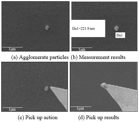
Since the carbon nanotube–silver nanocluster structure achieves the function of replacing copper wires on the electrode substrate in practical applications, the construction of carbon nanotube–silver nanocluster particle structure on the electrode substrate should be experimentally verified. AFM probes are used to pick up well-dispersed silver nanoclusters on ITO conductive glass substrates, and the diameter of the silver nanoclusters measured is approximately 200 nm.
As shown in Fig. 12, it can be observed that the AFM probe stably picks up the selected silver nanoclusters particles; then the carbon nanotubes are dispersed on the electrode substrate with appropriate dispersion parameters, and the gold substrate is selected under the observation of the scanning electron microscope. The length and diameter of the carbon nanotubes are 3.4 µm and 104 nm, respectively. The picked silver nanocluster particles are placed at one end of the selected carbon nanotubes to complete the construction of the carbon nanotube–silver nanocluster particle structure.
In Fig. 13, it can be observed that due to the long duration of the placement process, the carbon nanotubes in the upper right corner undergo ablation and leave a blackish mark on the substrate in an environment where the electron beam is continuously emitted, and the same situation occurs at the end where the carbon nanotubes are operated. The reason is that the structure of the carbon nanotubes becomes more fragile in an environment where the scanning electron beam is continuously emitted, and the repeated friction of the probe on the substrate crushes some of the carbon nanotubes leaving a black trail.
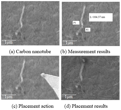
Figure 13Construction of carbon nanotube–nanocluster cluster structure at electrode substrate in three dimensions.
The silver nanocluster particles were deformed in the process of being picked up by the AFM probe, the two parts of the clusters adhered to the AFM probe, and the adhesion position was on the side of the AFM probe tip. Analysis of the above experimental results leads to the following conclusions.
-
AFM probes can pick up smaller silver nanoclusters in three dimensions, and as the particle size increases, the silver nanocluster will deform or even partially detach, at which point the remaining parts can be picked up twice in the same way to complete the pickup of the silver nanocluster particles.
-
Silver nanoparticles are adsorbed on the side of the AFM probe tip, which is a more suitable location for anchoring silver nanocluster particles to the end points of carbon nanotubes by pushing and pulling in the substrate plane.
-
The silver nanocluster particles were stabilized on the end points of the carbon nanotubes by the Van der Waals force, and the size and shape of the nanocluster particles did not change significantly during the placement process.
-
After placement, the nanocluster particles do not move with the withdrawal of the AFM probe, and the particles bind to the carbon nanotubes and stabilize, so as to achieve cross-substrate relocation to build the carbon nanotube–nanocluster particle structure.
The three-dimensional construction of carbon nanotube–silver nanocluster particle structures is completed, and the feasibility of three-dimensional manipulation of nanocluster particles is verified.
With the rapid development of nanotechnology, the size of electronic components continues to break through the limit. Therefore, higher requirements are put forward for nanoparticle manipulation technology, especially nanoparticle manipulation technology. This paper conducts theoretical analysis and experimental research on nanoparticle manipulation. This paper analyzed the dynamic process of driving nanoparticles, adsorbing nanoparticle and adsorbing nanocluster particles by the probe. The simulation shows that when the nanoparticle is driven by the probe, the friction between nanoparticle and substrate is affected by the contact area. The nanoparticle manipulation experiments were carried out under the SEM nanoparticle manipulation platform, where silver nanocluster particles were picked up across the substrate and placed on one end of the carbon nanotubes on the gold substrate to complete the three-dimensional construction of carbon nanotube–silver nanocluster particles. In this paper, the smallest unit of the carbon nanotube wire is constructed by the experiment of building carbon nanotube–nanocluster particle structure by three-dimensional operation, which lays the foundation for carbon nanotube interconnection technology.
No data sets were used in this article.
ZY and LY established an overall paper research framework. XL and JL conducted detailed optimization and data experiments on the overall paper. XL and YD contributed to manuscript writing and data collection and analysis. LY and YW carried out paper revisions and financial support of the paper.
The authors declare that they have no conflict of interest.
This article is part of the special issue “Robotics and advanced manufacturing”. It is not associated with a conference.
The authors are grateful to the National Key R&D Program of China.
This research has been supported by the National Key R&D Program of China (grant no. 2017YFB1104900).
This paper was edited by BO LI and reviewed by four anonymous referees.
Bartenwerfer, M. and Fatikow, S.: Nanorobot-based handling and transfer of individual silicon nanowires, Int. J. Intell. Mech. Robot., 2, 34–46, https://doi.org/10.4018/ijimr.2012040103, 2012.
Bocko, J. and Lengvarský, P.: Buckling of single-walled carbon nanotubes with and without defects, J. Mech. Sci. Technol., 31, 1825–1833, https://doi.org/10.1007/s12206-017-0330-y, 2017.
Bocko, J., Lengvarský, P., Huňady, R., and Šarloši, J.: The computation of bending eigenfrequencies of single-walled carbon nanotubes based on the nonlocal theory, Mech. Sci., 9, 349–358, https://doi.org/10.5194/ms-9-349-2018, 2018.
Conradi, M., Kocijan, A., Kosec, T., and Podgornik, B.: Manipulation of TiO2 Nanoparticle/Polymer Coatings Wettability and Friction in Different Environments, Materials, 13, 1702, https://doi.org/10.3390/ma13071702, 2020.
Fukuda, T., Arai, F., and Dong, L.: Assembly of nanodevices with carbon nanotubes through nanorobotic manipulations, P. IEEE, 91, 1803–1818, https://doi.org/10.1109/JPROC.2003.818334, 2003.
Fukuda, T., Arai, F., and Dong, L.: Nanorobotic systems, Int. J. Adv. Robot. Syst., 2, 264–275, https://doi.org/10.5772/5778, 2005.
Komissarenko, F., Zograf, G., Makarov, S., Petrov, M., and Mukhin, I.: Manipulation Technique for Precise Transfer of Single Perovskite Nanoparticles, Nanomaterials, 10, 1306, https://doi.org/10.3390/nano10071306, 2020.
Maugis, D.: Adhesion of sphere: the JKR-DMT transition using a Dugdale mode, J. Colloid Interf. Sci, 150, 243–269, https://doi.org/10.1016/0021-9797(92)90285-T, 1992.
Mohsin, K. M., Srivastava, A., Sharma, A. K., and Mayberry, C.: A thermal model for carbon nanotube interconnects, Nanomaterials, 3, 229–241, https://doi.org/10.3390/nano3020229, 2013.
Robinson, M. T. A. and Adali, S.: Buckling of elastically restrained nonlocal carbon nanotubes under concentrated and uniformly distributed axial loads, Mech. Sci., 10, 145–152, https://doi.org/10.5194/ms-10-145-2019, 2019.
Ru, C., Zhang, Y., Sun, Y., Zhong, Y., Sun, X., Hoyle, D., and Cotton, I.: Automated four-point probe measurement of nanowires inside a scanning electron microscope, IEEE T. Nanotechnol., 10, 674–681, https://doi.org/10.1109/TNANO.2010.2065236, 2010.
Shi, Q., Yang, Z., Guo, Y., Wang, H., Sun, L., Huang, Q., and Fukuda, T.: A vision-based automated manipulation system for the pick-up of carbon nanotubes, IEEE/ASME Trans. Mech., 22, 845–854, https://doi.org/10.1109/TMECH.2017.2649681, 2017.
Shu, Y., Kang, Z., and Zhengtian, X.: Strong and High-Precision Manipulation of Nanoparticle with Graphene-Coated Fiber Systems, Plasmonics, 14, 1377–1384, https://doi.org/10.1007/s11468-514 019-00922-z, 2019.
Stergar, J. and Osterman, N.: Thermophoretic tweezers for single nanoparticle manipulation, Beilstein J. Nanotech., 11, 1126–1133, https://doi.org/10.3762/bjnano.11.97, 2020.
Wang, Z., Liu, L., Wang, Y., Wang, Z., Xi, N., Hou, J., Wang, W., and Yuan, S.: Stable Nanomanipulation Using Atomic Force Microscopy: A virtual nanohand for a robotic nanomanipulation system, IEEE Nanotechnology Magazine, 7, 6–11, https://doi.org/10.1109/MNANO.2013.2289693, 2013.
Williams, P. A., Papadakis, S. J., Falvo, M. R., Patel, A. M., Sinclair, M., Seeger, A., Helser, A., Taylor, R. M. Washburn, S., and Superfine, R.: Controlled placement of an individual carbon nanotube onto a microelectromechanical structure, Appl. Phys. Lett., 80, 2574–2576, https://doi.org/10.1063/1.1467701, 2002.
Yang, Z., Chen, T., Wang, Y., Sun, L., and Fukuda, T.: Carbon nanotubes pickup by van der Waals force based on nanorobotics manipulation inside SEM, Micro Nano Lett., 11, 645–649, https://doi.org/10.1049/mnl.2016.0287, 2016.
Yu, N., Nakajima, M., Shi, Q., Yang, Z., Wang, H.P., Sun, L. N., Huang, Q., and Fukuda, T.: Characterization of the resistance and force of a carbon nanotube/metal side contact by nanomanipulation, Scanning, 5910734, https://doi.org/10.1155/2017/5910734, 2017a.
Yu, N., Shi, Q., Nakajima, M., Wang, H., Yang, Z., Sun, L. N., Huang, Q., and Fukuda, T.: 3D assembly of carbon nanotubes for fabrication of field-effect transistors through nanomanipulation and electron-beam-induced deposition, J. Micromech. Microeng., 27, 105007, https://doi.org/10.1088/1361-6439/aa7961, 2017b.
Yuan, S., Wang, Z., Xi, N., Wang, Y., and Liu, L.: AFM tip position control in situ for effective nanomanipulation, IEEE/ASME Trans. Mech., 23, 2825–2836, https://doi.org/10.1109/TMECH.2018.2868983, 2018.
Zhang, Y. L., Zhang, Y., Ru, C., Chen, B. K., and Sun, Y.: A load-lock-compatible nanomanipulation system for scanning electron microscope, IEEE/ASME Trans. Mech., 18, 230–237, https://doi.org/10.1109/TMECH.2011.2166162, 2011.
Zimmermann, S., Tiemerding, T., and Fatikow, S.: Automated robotic manipulation of individual colloidal particles using vision-based control, IEEE/ASME Trans. Mech., 20, 2031–2038, https://doi.org/10.1109/TMECH.2014.2361271, 2014.